


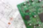
PCBA Process and Technology
- Phillip Tran
- Dec 21, 2022
- 7 min read
In the following article, we will look at the different methods utilized during the PCBA process for adding and securing components in a manner that allows them to function and communicate to achieve the desired functionality and durability. i-Tech e-Services is committed to keeping our clients informed so that they are assured every step to create the highest quality product and the most efficient production methods are exercised. State of the art machinery, thorough inspection processes, and prototype consultation are a few of the aspects that allow our experts to save our clients time and money while maintaining the highest standards of quality. Join us as we learn a little more about the journey a PCB takes from prototype to functional product ready for mass production and implementation.
The PCBA procedure cannot start until a few prerequisite stages have been completed. This mostly consists of a DFM check, which stands for design for manufacturability check, and aids PCB producers in determining how effectively a PCB design functions.
The manufacturer typically needs the PCB design file, any additional design notes, and any special requirements to initiate a PCB assembly project. This makes it possible for the PCB assembly technicians to examine the PCB file for any problems that might restrict the PCB's functioning or manufacturing capability.
During this prototyping process, the PCBA company provides a critical role in lending expertise and vision to bring the desired creation to life that will function as intended and create a high-standard end product. At i-Tech e-Services, we have professionals who are well versed in helping find potential complications and improvements to design before production ever begins.
Each design criterion for the PCB will be examined during the DFM examination. This inspection pays close attention to any qualities that might be troublesome, superfluous, or altogether absent. Each of these problems has the potential to drastically lower the project's final success rate. A common issue is found in the layout of the PCB components which can have a great effect on the performance.
The DFM checks have the ability to help correctly evaluate a project and confirm its functional accuracy. By doing these checks, it allows for i-Tech to save its clients valuable time and money before any physical steps are taken. By having expert help during the planning stages, labor and actual production materials can be utilized to their fullest and not wasted on what are sometimes small and hard to detect flaws in the PCB prototype design. Our technicians have the knowledge and industry level experience to be able to swiftly detect any areas of improvement or adjustments that may need to be implemented.
Once this is complete the design is ready to be produced. There are multiple steps in the actual production to get from a PCB free of components to a finished functional product ready for reproduction.
Initial Process for Mounting SMDs
As part of PCB assembly, solder paste is first put on the board. This procedure, which is similar to screen printing on clothing, involves covering the PCB with a thin stainless steel stencil. Assemblers can currently only apply solder paste to areas of the PCB specified by the applied stencil. On the final PCB, these locations will represent the component positions.

The solder paste is made up of small spheres of solder contained within flux to create the needed paste. The solder can be made up of various metals but a common combination used to create the solder in solder paste includes approximately 96.5 percent of tin, followed by silver (3%) and copper (0.5%). Flux, the material that holds the solder in a paste form, is mixed with the solder to aid in melting and surface adhesion. Solder paste is a gray substance that needs to be placed on the board in incredibly specific locations and amounts.
The PCB will be inserted, with the stencil in place, into an automated machine that will precisely apply the solder paste with precision. The paste is applied to the stencil by the machine in an equal layer, covering all the empty spaces. As the stencil is removed the solder paste will stay in place.

Secondary Process for Mounting SMDs
Surface-mount devices, or SMDs, are placed on a ready PCB by a robotic apparatus after the solder paste has been applied. The next stage in the PCBA process is to securely adhere these SMDs to the board's surface.
Originally, technicians would place each component by hand. However, as technology advanced, this process was taken over by robotics which allowed for increased speed, accuracy, and endurance. This shift would drastically change the pace of output and consistency in the PCBA process.
During the PCBA process, the solder-pasted PCB is transported to a pick and place machine. The machine analyzes and aligns the PCB and begins selecting and delivering the various SMDs to their correct location as predetermined by the design into the solder paste. The components are inserted via rolls into loading stations on the pick and place machine allowing the machine to apply many different types of SMDs quickly and accurately onto a PCB, which creates the potential for production and efficiency that was impossible before the creation of this technological advancement.

Tertiary Process for Mounting SMDs
To allow the solder to set up and connect the components properly, a process called reflow soldering must take place. This process allows for the solder to be heated until it becomes molten creating permanent connections.
The PCB board is then placed on a conveyor belt after being picked and placed. The conveyor belt pulls the PCB at a controlled speed through a long tunnel shaped oven. Utilizing multiple controlled heaters the oven will reach up to 250 degrees Celsius, or 480 degrees Fahrenheit gradually to achieve the perfect solder state.

The PCB is placed back in the oven after the solder has melted. During this phase, the heaters are at a lower temperature allowing the solder to properly solidify creating strong and reliable connections. The SMDs are consequently permanently joined to the PCB by a solder connection.
If the PCBA process is specifically for a two-sided PCB, then additional consideration must be taken. Whichever side has the lesser number of components will be sent through the process of stenciling, SMT mounting, and the reflow before the more complicated side is commenced.
Final Process for Mounting SMDs
After the reflow procedure, the surface mount components must be soldered into place, and the final PCBA and assembled board must be checked for operation. Movement during reflow frequently causes a link to be lost whole or partially. This movement linking circuit elements that shouldn't be connected might occasionally cause shorts.
Any of the several inspection techniques can be used to look for these mistakes and misalignments. Technicians have several skills and tools at their disposal to ensure accuracy and the absence of defects. An overview of the most common methods includes:
• Manual Checks: Even with advancements in robotics and overall technology, manual checks are still crucial to ensuring the process is working properly and no mistakes are being replicated before and during mass production. No matter the size of production from small to large volume, manual checks provide a substantial effect on quality control.
• Automatic Optical Inspection: A more complex strategy is needed for PCBs in larger batches. Every soldered component is examined by the sophisticated cameras on an AOI machine, also known as an autonomous optical inspection machine. The cameras can detect differences in the way the solder connections reflect light and report any insufficient connections. These devices have a tremendous amount of processing power, which allows for the fast inspection of several boards.
• X-ray inspection: Occasionally, layers, including see-through layers, are examined with X-rays to look for any potential faults that might not be immediately obvious.

After the inspection process, the technicians will evaluate if any problems can be corrected or if a new board is needed. The process will then move on to testing the components to ensure they function as intended. The reliability of the PCB connections must be thoroughly checked. For boards that need calibration or programming, extra precautions are taken to ensure optimal performance.
These inspections and analyses are integral procedures to ensure that the PCB will function as intended and all the connections are durable and reliable.
PTH Components
In addition to the typical SMDs, the type of board covered by PCBA may have a variety of other components. PTH components, also known as plated through-hole components, are among them.
A PCB hole that has plating across the entire board is referred to as a plated through hole. Due to the opening created by a PTH, soldering paste is an ineffective manner of adhering components. To ensure that these connections can transmit the necessary signals on the PCB, a more sophisticated sort of soldering technique in substitution of solder paste:

• Hand through-hole insertion, which requires manual soldering, is a simple procedure. In many situations when manual insertion occurs, an assembly line of individuals responsible for connecting one specific part each would be utilized. For every PTH that requires outfitting, the procedure is repeated. Depending on how many PTH components must be installed during a PCBA cycle, this procedure could take some time. Despite the added time and degree of technicality involved with utilizing PTH components, they are still frequently used in PCB designs.
• Soldering in a wave: This automated soldering method differs greatly from human soldering. The board is then placed on yet another conveyor line following the installation of the PTH component. This time, a wave of molten solder is applied to the bottom of the board as the conveyor belt travels through a specialized oven. Each pin on the board's underside is soldered during this process.
For double-sided PCBs, this kind of soldering is practically impossible because doing so would leave any delicate electrical components worthless.
When the soldering procedure is complete, the PCB will either go through a final inspection or repeat the prior procedures if additional parts need to be added or another side needs to be finished.
Functionality Testing and Final Inspection
The PCB will undergo a functional test after the soldering phase of the PCBA process is complete. The functional test will be used to put the PCB through a series of tasks that as one might infer from the name will test the PCB to ensure it operates as it is intended to function. Technicians will apply power and create various input signals that would be expected in a post-production user interaction. They will evaluate the results and report on any issues for correction or approve it as successful. The PCB fails the test if any feature such as voltage, current, or signal output, exhibits unacceptable fluctuation or reaches peaks outside of a predetermined range.
Inspection and interval testing are key to any production's success. If these steps are overlooked or rushed it can be catastrophic for the end product’s functionality. This is why it is absolutely crucial to choose a partner that commits itself to integrity and the highest standards of operation. i-Tech e-Service has a proven track record of providing clients with unmatched professionalism and consistency. At i-Tech our clients can be focused on design and roll-out while feeling ensured that the production process is taking place with the utmost care and proficiency.